
具体描述
内容简介
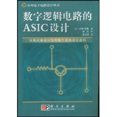
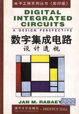
市面上虽然已有许多关于数字集成电路设计的书籍,但
绝大部分都是孤立地讨论“数字系统”、或“数字电路单元”、
或“设计方法”。而本书则将系统、电路和设计方法这三者
有机地结合起来,深入地讨论了CMOS、双极型和砷化镓
(GaAS)数字集成电路。本书在详细介绍集成电路的器件模型
和墓本单元电路的基础上,系统地介绍了数字集成电路系统
设计中的四类关键技术:运算单元设计、时序组织与规划、
存储单元、互连线与寄生效应,是一本内容丰富,且特别
适合于深亚微米数字集成电路设计的优秀教材。
作者简介
目录信息
Chapterl: Introduction
1.1 A Historical Perspective
1.2 Issues in Digital Integrated Circuit Design
1.3 To Probe Further
1.4 Exercises
PART 1: A CIRCUIT PERSPECTIVE
Chapter 2: The Devices
2.1 Introduction
2.2 The Diode
2.2.1 A First Glance at the Device
2.2.2 Static Behavior
2.2.3 Dynamic, or Transient, Behavior
2.2.4 The Actual Diode-Secondary Effects
2.2.5 The SPICE Diode Model
2.3 The MOS(FET) Transistor
2.3.1 A First Glance at the Device
2.3.2 Static Behavior
2.3.3 Dynamic Behavior
2.3.4 The Actual MOS Transistor-Secondary Effects
2.3.5 SPICE Models for the MOS Transistor
2.4 The Bipolar Transistor
2.4.1 A First Glance at the Device
2.4.2 Stalic Behavior
2.4.3 Dynamic Behavior
2.4.4 The Actual Bipolar Transistor-Secondary Effects
2.4.5 SPICE Models for the Bipolar Transistor
2.5 A Word on Process Variations
2.6 Perspective: Future Device Developments
2.7 Summary
2.8 To Probe Further
2.9 Exercises and Design Problems
Appendlx A: Layout Design Rules
Appendlx B: Small-Slgnal Models
Chapter 3: The Inverter
3.1 Introduction
3.2 Delinitions and Properties
3.2.1 Area and Complexity
3.2.2 Functionality and Robustness: The Static Behavior
3.2.3 Performance: The Dynamic Behavior
3.2.4 Power and Energy Consumption
3.3 The Static CMOS Invener
3.3.1 A First Glance
3.3.2 Evaluating the Robustness of the CMOS Inverter: The Static Behavior
3.3.3 Perfonnance of CMOS Inverter: The Dynamic Behavior
3.3.4 Power Consumption and Power-Delay Product
3.3.5 A Look into the Future: Effects of Technology Scaling
3.4 The Bipolar ECL Inverter
3.4.1 Issues in Bipolar Digital Design: A Case Study
3.4.2 The Emitter-Coupled Logic (ECL) Gate at a Glance
3.4.3 Robustness and Noise Immunity: The Steady-State Characteristics
3.4.4 ECL Switching Speed: Thc Transient Behavior
3.4.5 Power Consumption
3.4.6 Looking Ahead: Scaling the Technology
3.5 Perspective: Area, Perfonnance, and Dissipation
3.6 Summary
3.7 To Probe Further
3.8 Exercises and Design Problems
Chapter 4: Designing Combinational Logk Cates in CMOS
4.1 Introduction
4.2 Static CMOS Design
4.2.1 Complementary CMOS
4.2.2 Ratioed Logic
4.2.3 Pass-Transistor Logic
4.3 Dynamic CMOS Design
4.3.1 Dynamic Logic: Basic Principles
4.3.2 Perfonnance of Dynamic Logic
4.3.3 Noise Considerations in Dynamic Design
4.3.4 Cascading Dynamic Gates
4.4 Power Consumption in CMOS Gates
4.4.1 Switching Activity of a Logic Gate
4.4.2 Glitching in Static CMOS Circuits
4.4.3 Short-Circuit Currents in Static CMOS Circuits
4.4.4 Analyzing Power Consumption Using SPICE
4.4.5 Low-Power CMOS Design
4.5 Perspective: How to Choose a Logic Style
4.6 Summary
4.7 To Probe Further
4.8 Exercises and Design Problems
Appendix C: Layout Techniques for Complex Cates
Chapter 5: Very High Perfonnance Digital Circuits
5.1 Introduction
5.2 Bipolar Gate Design
5.2.1 Logic Design in ECL
5.2.2 Differential ECL
5.2.3 Current Mode Logic
5:2.4 ECL with Active Pull-Downs
5.2.5 Altemative Bipolar Logic Styles
5.3 The BiCMOS Approach
5.3.1 The BiCMOS Gate at a Glance
5.3.2 The Static Behavior and Robustness Issues
5.3.3 Perfonnance of the BiCMOS Inverter
5.3.4 Power Consumption
5.3.5 Technology Scaling
5.3.6 Designing BiCMOS Digital Gates
5.4 Digital Gallium Arsenide Design *
5.4.1 GaAs Devices and Their Properties
5.4.2 GaAs Digital Circuit Design
5.5 Low-Temperature Digital Circuits *
5.5.1 Low-Temperature Silicon Digital Circuits
5.5.2 Superconducting Logic Circuits
5.6 Perspective: When to Use High-Performance Technologies
5.7 Summary
5.8 To Probe Further
5.9 Exercises and Design Problems
Appendlx D: The Schottky-Bamer Oiode
Chapter 6: Designing Sequential Logic Circuits
6.1 Introduction
6.2 Static Sequential Circuits
6.2.1 Bistability
6.2.2 Flip-Flop Classification
6.2.3 Master-Slave and Edge-Triggered FFs
6.2.4 CMOS Static Flip-Flops
6.2.5 Bipolar Static Flip-Flops
6.3 Dynamic Sequentia) Circuits
6.3.1 The Pseudostatic Latch
6.3.2 The Dynamic Two-Phase Flip-Flop
6.3.3 The C2MOS Latch
6.3.4 NORA-CMOS-A Logic Style for Pipelined Structures
6.3.5 True Single-Phase Clocked Logic (TSPCL)
6.4 Non-Bistable Sequential Circuits
6.4.1 The Schmitt Trigger
6.4.2 Monostable Sequential Circuits
6.4.3 Astable Circuits
6.5 Perspective: Choosing a Clocking Strategy
6.6 Summary
6.7 To Probe Funher
6.8 Exercises and Design Problems
PART 11: A SYSTEMS PERSPECTIVE
Chapter 7: Designing Arithmetic Building Blocks
7.1 Introduction
7.2 Datapaths in Digital Processor Architectures
7.3 The Adder
7.3.1 The Binary Adder: Definitions
7.3.2 The Full Adder: Circuit Design Considerations
7.3.3 The Binary Adder: Logic Design Considerations
7.4 The Multiplier
7.4.1 The Multiplier: Definitions
7.4.2 The Array Multiplier
7.4.3 Other Multiplier Structures
7.5 The Shifter
7.5.1 BarrelShifter
7.5.2 Logarithmic Shifter
7.6 Other Arithmetic Operators
7.7 Power Considerations in Datapath Structures
7.7.1 Reducing the Supply Voltage
7.7.2 Reducing the Effective Capacitance
7.8 Perspective: De.sign as aTrade-off
7.9 Summary
7.10 To Probe Further
7.11 Exercises and Design Problems
Appendix E: From Datapath Schematics to Layout
Chapter 8: Coping wlth Interconnect
8.1 Introduction
8.2 Capacitive Parasitics
8.2.1 Modeling Interconnect Capacitance
8.2.2 Capacitance and Reliability-Cross Talk
8.2.3 Capacitance and Performance in CMOS
8.2.4 Capacitance and Performance in Bipolar Design
8.3 Resistive Parasitics
8.3.1 Modeling and Scaling of Interconnect Resistance
8.3.2 Resistance and Reliability-Ohmic Voltage Drop
8.3.3 Electromigration
8.3.4 Resistance and Performance-RC Delay
8.4 Inductive Parasitics
8.4.1 Sources of Parasitic Inductances
8.4.2 Inductance and Reliability- Voltage Drop
8.4.3 Inductance and Performance-Transmission Lin5e Effects
8.5 Comments on Packaging Technology
8.5.1 Package Materials
8.5.2 Interconnect Levels
8.5.3 Thennal Considerations in Packaging
8.6 Perspective: When to Consider Interconnect Parasitics
8.7 Chapter Summary
8.8 To Probe Further
8.9 Exercises and Design Problems
Chapter 9: Timing Issues in Digital Circuits
9.1 Introduction
9.2 Clock Skew and Sequential Circuit Performance
9.2.1 Single-Phase Edge-Triggered Clocking
9.2.2 Two-Phase Master-Slave Clocking
9.2.3 Other Clocking Styles
9.2.4 How to Counter Clock Skew Problems
9.2.5 Case Study-The Digital Alpha 21164 Microprocessor
9.3 Self-Timed Circuit Design*
9.3.1 Selt-Timed Concept
9.3.2 Completion-Signal Generation
9.3.3 Self-Timed Signaling
9.4 Synchronizers and Arbiters*
9.4.1 Synchronizers-Concept and Implementation
9.4.2 Arbiters
9.5 Clock Generation and Synchronization*
9.5.1 Clock Generators
9.5.2 Synchronization at the System Level
9.6 Perspective: Synchronous versus Asynchronous Design
9.7 Summary
9.8 To Probe Further
9.9 Exerci.ses and Design Problems
Chapter 10: Designing Memory and Array Structures
10.1 Introduction
10.2 Semiconductor Memories--An Introduction
10.2.1 Memory Classification
10.2.2 Memory Architectures and Building Blocks
10.3 The Memory Core
10.3.1 Read-Only Memories
10.3.2 Nonvolati le Read-Write Memories
10.3.3 Read-Write Memories (RAM)
10.4 Memory Peripheral Circuitry
10.4.1 The Address Decoders
10.4.2 Sense Amplifiers
10.4.3 Drivers/Buffers
10.4.4 Timing and Control
10.5 Memory Reliability and Yield
10.5.1 Signal-To-Noise Ratio
10.5.2 Memory yield
10.6 Case Studies in Memory Design
10.6.1 The Programmable Logic Array (PLA)
10.6.2 A 4 Mbit SRAM
10.7 Perspective: Semiconductor Memory Trends and Evolutions
10.8 Summary
10.9 To Probe Further
10.10 Exercises and Design Problems
Chapterll: Deslgn Methodologles
11.1 Introduction
11.2 Design Analysis and Simulation
11.2.1 Representing Digital Data as a Continuous Entity
11.2.2 Representing Data as a Discrete Entity
11.2.3 Using Higher-Level Data Models
11.3 Design Verification
11.3.1 Electrical Verification
11.3.2 Timing Verification
11.3.3 Functional (or Fonnal) Verification
11.4 Implementation Approaches
11.4.1 Custom Circuit Design
11.4.2 Cell-Based Design Methodology
11.4.3 Anay-Based Implementation Approaches
11.5 Design Synthesis
11.5.1 Circuit Synthesis
11.5.2 Logic Synthesis
11.5.3 Architecture Synthesis
11.6 Validation and Testing of Manufactured Circuits
11.6.1 TestProcedure
11.6.2 Design for Testability
11.6.3 Test-Pattem Generation
11.7 Perspective and Summary
11.8 To Probe Further
11.9 Exercises and Design Problems
Problem Solutions
· · · · · · (收起)
读后感
要读这本书,我觉得得要有三个前提。第一:不急躁的心态,第二:有层次想当的人可以讨论;第三:比较深厚的数字电路的基础。这可能是由于国外的教学方式与国内的教学方式不同,所以造成了国外教材在国内并不被很多学生所接受的原因之一。国外是一种讨论式、引导式的教学方式,...
评分要读这本书,我觉得得要有三个前提。第一:不急躁的心态,第二:有层次想当的人可以讨论;第三:比较深厚的数字电路的基础。这可能是由于国外的教学方式与国内的教学方式不同,所以造成了国外教材在国内并不被很多学生所接受的原因之一。国外是一种讨论式、引导式的教学方式,...
评分要读这本书,我觉得得要有三个前提。第一:不急躁的心态,第二:有层次想当的人可以讨论;第三:比较深厚的数字电路的基础。这可能是由于国外的教学方式与国内的教学方式不同,所以造成了国外教材在国内并不被很多学生所接受的原因之一。国外是一种讨论式、引导式的教学方式,...
评分要读这本书,我觉得得要有三个前提。第一:不急躁的心态,第二:有层次想当的人可以讨论;第三:比较深厚的数字电路的基础。这可能是由于国外的教学方式与国内的教学方式不同,所以造成了国外教材在国内并不被很多学生所接受的原因之一。国外是一种讨论式、引导式的教学方式,...
评分要读这本书,我觉得得要有三个前提。第一:不急躁的心态,第二:有层次想当的人可以讨论;第三:比较深厚的数字电路的基础。这可能是由于国外的教学方式与国内的教学方式不同,所以造成了国外教材在国内并不被很多学生所接受的原因之一。国外是一种讨论式、引导式的教学方式,...
用户评价
有讲到完整的电路设计流程,清华教材之一
评分研究生读过的书。。。。
评分研究生读过的书。。。。
评分有讲到完整的电路设计流程,清华教材之一
评分研究生读过的书。。。。
相关图书
本站所有内容均为互联网搜索引擎提供的公开搜索信息,本站不存储任何数据与内容,任何内容与数据均与本站无关,如有需要请联系相关搜索引擎包括但不限于百度,google,bing,sogou 等
© 2026 book.quotespace.org All Rights Reserved. 小美书屋 版权所有

